- 您现在的位置:买卖IC网 > Sheet目录362799 > EVAL-AD1928EB (Analog Devices, Inc.) 2 ADC/8 DAC with PLL, 192 kHz, 24-Bit Codec
AD1928
ABSOLUTE MAXIMUM RATINGS
Rev. 0 | Page 8 of 32
Table 8.
Parameter
Analog (AVDD)
Digital (DVDD)
Input Current (Except Supply Pins)
Analog Input Voltage (Signal Pins)
Digital Input Voltage (Signal Pins)
Operating Temperature Range (Case)
Storage Temperature Range
Rating
0.3 V to +3.6 V
0.3 V to +3.6 V
±20 mA
–0.3 V to AVDD + 0.3 V
0.3 V to DVDD + 0.3 V
40°C to +125°C
65°C to +150°C
Stresses above those listed under the Absolute Maximum
Ratings may cause permanent damage to the device. This is a
stress rating only; functional operation of the device at these or
any other conditions above those indicated in the operational
section of this specification is not implied. Exposure to absolute
maximum rating conditions for extended periods may affect
device reliability.
THERMAL RESISTANCE
θ
JA
represents thermal resistance, junction-to-ambient;
θ
JC
represents the thermal resistance, junction-to-case. All
characteristics are for a 4-layer board.
Table 9. Thermal Resistance
Package Type
48-Lead LQFP
θ
JA
50.1
θ
JC
17
Unit
°C/W
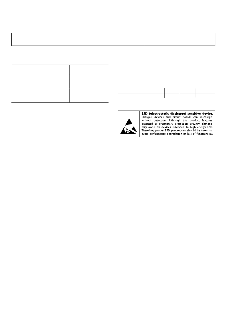
ESD CAUTION
发布紧急采购,3分钟左右您将得到回复。
相关PDF资料
EVAL-AD1938EB
4 ADC/8 DAC with PLL, 192 kHz, 24 Bit CODEC
EVAL-AD1939EB
4 ADC/8 DAC with PLL, 192 kHz, 24 Bit CODEC
EVAL-AD1935EB
4 ADC/8 DAC with PLL, 192 kHz, 24 Bit CODEC
EVAL-AD1936EB
4 ADC/8 DAC with PLL, 192 kHz, 24 Bit CODEC
EVAL-AD1937EB
4 ADC/8 DAC with PLL, 192 kHz, 24 Bit CODEC
Eval-AD1940EB
SigmaDSP-TM Multichannel 28-Bit Audio Processor
EVAL-AD1953EB
16-bit fixed point DSP with Flash
EVAL-AD1958EB
PLL/Multibit DAC
相关代理商/技术参数
EVAL-AD1928EBZ
制造商:AD 制造商全称:Analog Devices 功能描述:2 ADC/8 DAC with PLL, 192 kHz, 24-Bit Codec
EVAL-AD1934EB
制造商:AD 制造商全称:Analog Devices 功能描述:8-Channel DAC with PLL, 192 kHz, 24 Bits
EVAL-AD1935EB
制造商:AD 制造商全称:Analog Devices 功能描述:4 ADC/8 DAC with PLL, 192 kHz, 24 Bit CODEC
EVAL-AD1936EB
制造商:AD 制造商全称:Analog Devices 功能描述:4 ADC/8 DAC with PLL, 192 kHz, 24 Bit CODEC
EVAL-AD1937AZ
功能描述:BOARD EVAL FOR AD1937 RoHS:是 类别:编程器,开发系统 >> 评估演示板和套件 系列:- 标准包装:1 系列:PSoC® 主要目的:电源管理,热管理 嵌入式:- 已用 IC / 零件:- 主要属性:- 次要属性:- 已供物品:板,CD,电源
EVAL-AD1937EB
制造商:AD 制造商全称:Analog Devices 功能描述:4 ADC/8 DAC with PLL, 192 kHz, 24 Bit CODEC
EVAL-AD1937EBZ
制造商:Analog Devices 功能描述:EB SINGLE CHIP CODEC 4 ADC'S W/DIFF OUTP - Boxed Product (Development Kits)
EVAL-AD1938AZ
功能描述:BOARD EVAL FOR AD1938 RoHS:是 类别:编程器,开发系统 >> 评估演示板和套件 系列:- 标准包装:1 系列:PSoC® 主要目的:电源管理,热管理 嵌入式:- 已用 IC / 零件:- 主要属性:- 次要属性:- 已供物品:板,CD,电源